MOSFETS differ from ordinary (Junction) FETS that in
the former the gate is physically insulated from the channel with an insulating
layer of Silicon dioxide so that no current can flow from the gate to the
channel under any circumstance.
There are two types of MOSFETs available; they are
called Depletion type MOSFETS and Enhancement type MOSFETS. The basic
structures of both types is similar except one important difference, that the
depletion MOSFET has a physically implanted channel where as in enhancement
type MOSFETS a temporary channel is induced
whenever necessary by applying an appropriate voltage between gate and the
source.
Operation
of an n-channel depletion type MOSFET
In the n- channel device shown in Figure 13, the
gate is made negative with respect to the source, which has the effect of
creating a depletion area, free from charge carriers, beneath the gate. This
restrict the depth of the conducting channel, so increasing channel resistance
and reducing current flow through the device.
Of the two the enhancement type MOSFET is the
most widely used field effect transistor, especially in digital electronics,
and therefore our discussion is restricted to the enhancement type MOSFET.
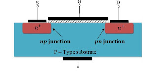
The
transistor is fabricated on a p-type substrate which is a single crystal of
silicon. Two heavily doped n-type regions indicated in the figure as n+
Source and n+ Drain regions are created
in the substrate. A thin (0.1µm) layer of silicon dioxide which is an
excellent insulator, is grown on the surface of the substrate covering the area
between the source and the drain. Metal is deposited on top of the oxide layer
to form the gate electrode of the device. Metal contacts are also formed on the
source and the drain regions and also on the substrate, also known as the body.
Now it should be clear as to why this device is called
Metal-Oxide-Semiconductor FET. Note some modern devices use poly-silicon to
form the gate electrode, but still they are called MOSFETS.
Operation
of the device with no gate voltage
|
|
and
the source. See Figure 15. One diode is formed by the n+ source and p substrate
on the LHS and the other junction by the substrate and the n+ drain junction on
the RHS. These back-to- back diodes prevent current conduction from drain to
source when a voltage VDS is applied across the drain and the
source.
Now
consider a situation where the source is grounded and a variable positive
voltage (VGS) is applied to the gate as shown in Figure 15. The
positive voltage on the gate drive away the (free) holes in the p substrate
from the region just underneath the gate. These holes are pushed down words
into the substrate leaving behind a carrier depletion region. As the gate
voltage is increased the electrons from the two n+ regions as well as from the substrate are attracted to the
region just underneath the gate inducing a temporary electron channel (n-channel) connecting the two n+ region
(i.e. source and the drain), Now if a voltage is applied between the drain and
the source, current flows through this induced n region. The induced n region
thus forms an n channel for current
flow, and hence the structure shown in Figures 14 and 15 are called n-channel MOSFETs.
The
value of VGS at which a sufficient number of mobile electrons accumulate in the
channel region to form a conducting channel is called the threshold voltage. This value typically lies in the range 1 to 3 V.
In
this process the channel created by inverting the property of the substrate
from p type to n type. Hence this induced channel is also called an inversion layer.
It
should be realized now that a p-channel MOSFET can also be
constructed in the similar way by fabricating two p+ regions and a gate in an n-type
substrate. In this case a p-channel can be formed by applying a negative VGS
voltage across gate and the source with gate negative.


No comments:
Post a Comment